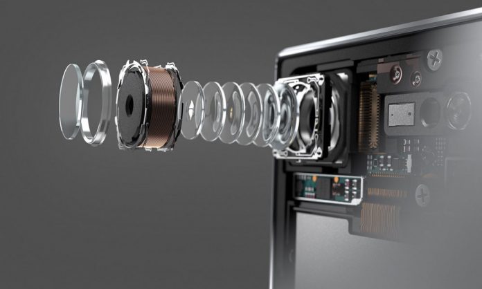
During its participation in the “IEDM 2019” conference, Samsung presented “14nm FinFET” technology, which will enable it to provide 144-megapixel high-resolution imaging sensors in the phones it will launch.
The new leaks around the upcoming Samsung sensor came via Ice Universe, where the new sensor comes with 144 megapixels and is based on FinFET architecture with an accuracy of 14 nm.
Sony is the largest competitor to the Korean giant, as it initially provided a 48-megapixel sensor for smartphones, and then Samsung achieved rapid development with the launch of a 64-megapixel sensor and another 108-megapixel, while Sony now stopped on its 64-megapixel sensor As Samsung prepares to add a new upgrade.
Energy consumption will also decrease by 37 percent when shooting 12-megapixel video, at a rate ranging from 30 to 120 fps.
On Twitter, an illustration posted on Ice Universe confirms Samsung’s 144-megapixel CMOS sensor, whereby the sensor integrates 100 million pixels to less than 10 million pixels, and a 14-nanometer resolution is also expected to support the sensor with a density of 100 Million pixels.
The Korean giant also reviewed improved imaging applications based on the 14-nanometer FinFET manufacturing process, but the company has not officially confirmed its plans to launch a 144-megapixel sensor.
On the other hand, Qualcomm presented its new processor, Snapdragon 865, with the support of a sensor with an accuracy of 200 megapixels, and with confirmation of leaks on Samsung’s support for the upcoming Galaxy S11 series with a sensor of 108 megapixels, we may witness the new upgrade in the sensor with the launch of the new versions of the Galaxy Note series.
Imaging sensor developers face a problem that requires high voltage work “2 volts and above”, while chip designers aim for the least effort to reduce energy consumption.


